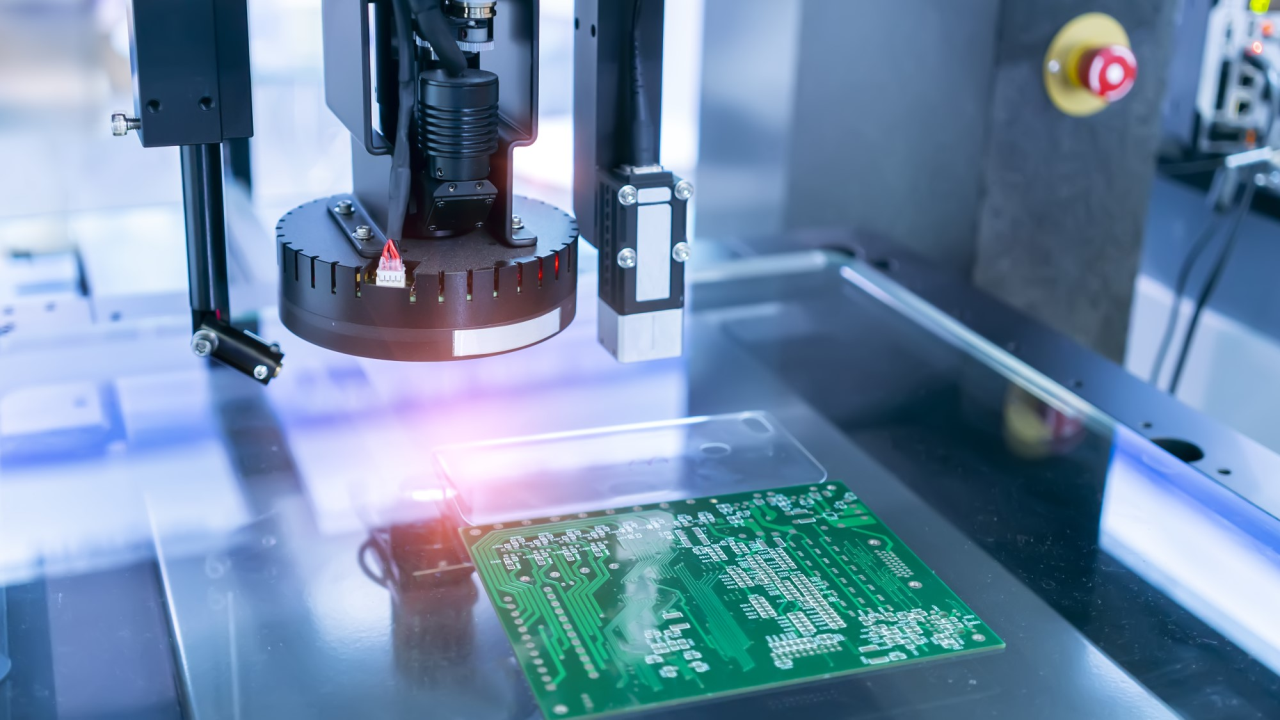
Importance Of AOI in PCB Manufacturing

As a visual quantitative and qualitative PCB test, Automated Optical Inspection (AOI) enables firms to lower the risk of human mistakes by decreasing their dependence on manual testing. AOI machine inspection services inspect PCBs to look for faults before sending them out for assembly. Furthermore, it gives real-time data on the efficiency of production lines and can assist businesses in avoiding costly manufacturing blunders.
What Does An AOI Reviews?
Defects in Soldering
Metal components on a PCB are connected using a low-melting-temperature alloy, such as lead-free tin or tin and lead alloy. Although it is comparable to welding, the metal components are not melted during the procedure. Soldering faults occur when the junctions between two metal components do not develop as expected.
AOI can check for the following frequent soldering defects:
- Open Circuits
Having an open circuit on your PCB is a typical concern, as an unfinished circuit hinders the flow of electrical current. The board won’t work correctly if a circuit is open.
Vias and traces that are not properly constructed or soldered incorrectly might lead to open circuits. An evident open circuit can be detected by eye examination or x-ray imaging in some cases, but AOI can identify even marginally open circuits and flag the board for correct circuit closure when necessary.
- Solder Bridges
In a PCB, solder bridges develop when the solder links two components on the board that is not supposed to be connected to each other. Overuse of solder in board fabrication or solder seepage into a region of the board meant to be solder-free can result in these bridges forming.
It is common for solder bridges to form when they do not separate from their leads before solidifying. These metal pads are called leads because they are meant to link two points on the circuit board.
Depending on the size of the leads, the amount of paste bonding them to the board, or the board’s pitch, solder may not detach from the board. When a solder bridge interferes with the intended current flow on a circuit, it can create serious problems.
They can short-circuit or burn out essential components or wires on the board. Fortunately, AOI scanning can detect even the tiniest solder bridges and return the defective boards for repairs. As a result, AOI testing is expected to generate $1,660 million in revenue by 2026.
- Insufficient Solder
A solder link with an inadequate amount of solder is the result of the manufacturing operation using too little solder to attach various components to the board. The board’s performance will suffer if the component interconnections are unstable due to improper soldering, leading to unstable electrical connections.
Similarly, if the proportion of solder on the board is so small that it cannot hold all of the components, the board would likely fail catastrophically. An AOI may scan the board and record the quantity of solder on each component, or it can compare the board to a reference picture to determine if it requires resoldering.
- Excess Solder
Too much solder is deposited on the circuit board during the manufacturing process. It might happen because the soldering tips are comprehensive or the solder has been overapplied. Several problems can arise from excessive soldering, including the creation of solder bridges.
Moreover, when a pin on the circuit board is overworked, and a huge spherical solder ball is formed, it is difficult to discern whether the pin is appropriately wetted.
A human inspector may miss one of these tiny solder balls for obvious reasons when inspecting hundreds of almost identical circuit boards. Excess solder may be quickly detected and sent back for rework with an iron or solder wick using an excellent AOI scanner.
Defects in Components
Defects in the minor functional components attached to a board are component defects. The following are some of the most prevalent PCB component defects:
- Lifted Lead
When one of the small metal pads on a PCB fails to attach correctly, a raised lead is formed. In some cases, extreme heat or handling during manufacture might cause a lead to be lifted. Leads that are overly long and rise when in contact with solder might also cause this problem.
Stability is an issue when a lead is raised. Your board’s pads provide connections to the copper plate below, but if the lead lifts, no connections can be made. Component failure and the board’s performance might be jeopardized by missing connections.
- Missing Components
Numerous factors might result in a PCB being devoid of an essential component. Components may be missing, or manufacturing may be interrupted due to poor soldering.
A PCB with a missing component is likely to fail catastrophically. A good AOI scanner is essential for detecting PCBs with missing components before they reach customers, even if the human eye can see them.
- Unaligned or Misplaced Component
Improperly placed components or elements that shift after placement can lead to misalignment or misplacement. The PCB may still function, but it may be sluggish due to a distorted or misplaced component. A reliable AOI scanner is vital for detecting even the slightest misalignments invisible to the human eye.


